Table Of Content

Whether it is a device that silently monitors vitals or a smartphone with an endless stream of notifications, all contain a PCB circuit board at the heart of their design. Over the years, printed circuit board manufacturing has continued to grow to keep up with the increasing demands of newer, faster, and more complex electronic circuitry. Discussions on the processes involved in devising and designing a PCB circuit board could fill a library, but here we will provide a surface-level introduction to the basics. A well-designed PCB layout can ensure that the traffic lights function properly and safely. The layout must take into account various factors such as the size and shape of the board, the placement of components, and the routing of the traces. The PCB must also be able to withstand harsh environmental conditions such as extreme temperatures, humidity, and vibration.
Extended data
Additionally, you can utilize the Altium Vault, which provides access to thousands of component libraries and adds flexibility to your project management and product development. However, you can also design your own schematic symbols and create footprints. Or, if you would like to take advantage of pre-existing component footprints, try using the Manufacturer Part Search Panel. To design and create PCBs, engineers and designers rely on Computer-Aided Design (CAD) tools.
Final Rules Check
While fiberglass-cored rigid PCBs are the most common PCBs on the market, they cannot and should not be used for every application out there — and there are some things they just can’t be used for. This is where other types of board, such as flexible and metal-cored boards, come into play. Flexible PCBs tend to be made out of bendable plastic that is capable of withstanding high — or in some cases low — temperatures, which makes it perfect for uses where PCBs and their components need to bend. Usually, PCB solder mask layers are green, but some manufacturers use different colors, such as red.
Step 6: Place Components
Proper thermal via and heat sink placement is critical for effective thermal management. Thermal vias should be placed as close to the heat source as possible, while heat sinks should be positioned to maximize their exposure to airflow and minimize obstruction from other components. In some cases, designers may also use thermal interface materials, such as thermal pads or thermal paste, to improve the thermal conductivity between the component and the heat sink. Proper impedance matching and termination are particularly important in high-speed digital circuits, where signal integrity is critical for reliable operation. By using controlled impedance traces and appropriate termination techniques, designers can minimize signal reflections, reduce distortion, and ensure that signals arrive at their destination with minimal degradation. The principles of PCB layout design involve several key considerations, including component placement, trace routing, and via placement.
These tools will operate on multiple nets simultaneously, making it easy to route a large number of traces in tandem. Over the next few pages, we'll discuss the composition of a printed circuit board, cover some terminology, a look at methods of assembly, and discuss briefly the design process behind creating a new PCB. The processes of printed circuit board fabrication and assembly are exact and demanding. To build a board so that its circuitry delivers the required performance means that manufacturers need precise design data to work from. Although the design and manufacturing of a PCB can be generalized as schematic capture, PCB layout, and circuit board fabrication and assembly, the details of each step are very involved. We’ll take a look here at some of the more specific aspects of each of these steps.
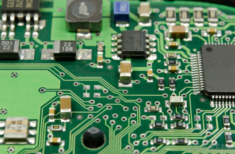
The printed circuit layout professional/profession in today’s industry now cross pollinates the necessary skill set between electrical, mechanical, software, test, and manufacturing disciplines. Understanding printed circuit boards (PCB) is a fundamental aspect of computer design. You’ll need to get accustomed to these green sheets and how they work if you ever hope to build a working computer or another electronic device. Today, standard designs can have many small components, such as tiny ICs, very small passive components, and advanced chips with very high pin counts. It's impossible to manually connect all of these components together with soldered wires, so the copper connections are deposited directly on insulating substrates as described in the above manufacturing process. Many of today's devices are advanced high density interconnect (HDI) designs with thousands of connections and multiple electrical interfaces, powering everything from smartphones to heart rate monitors to rockets.
Section 6 – PCB Design: Digital Routing
Before laying down any of your traces, be sure to use a trace width calculator (thanks, Advanced Circuits). Using this calculator will help you to easily determine how thick and wide all of your traces will need to be based on your specific design requirements. And if you end up having extra space on your board, go ahead and use traces with wider widths, as this won’t cost extra from your manufacturer. When placing your components always be mindful of how long your traces are going to need to be to connect your pins together.
PCBs play an important role in that they provide electrical interconnections between electronic components, rigid support to hold components, and a compact package that can be integrated into an end product. They are the main component in an electronic device that is responsible for form and function, and they allow advanced semiconductors to communicate with each other at very high data rates. Printed Circuit Board (PCB) design is like creating a blueprint that outlines the layout and connections of components on a circuit board. This process ensures that the final product functions as intended and meets the necessary specifications. The first step in PCB design is to gather the requirements and specifications for the circuit board.
It is important to note that it is not considered an assembly until all the required components are soldered on to the PWB. The fully assembled/populated PCB produces a fully functional ecosystem, which is where the metaphoric comparison between PCB design and designing a city is made. With Fusion 360, you’ll gain access to comprehensive electronics and PCB design tools in one software solution for electronics engineers. There’s a ton of work that goes into designing a printed circuit board. You likely invest a lot of your time making the perfect schematic or choosing the best parts. However, if you can’t get all of that data and theory down into something that functions in the real world, then what’s the point?
It is overlaid onto the copper layer to insulate the copper traces from accidental contact with other metal, solder, or conductive bits. This layer helps the user to solder to the correct places and prevent solder jumpers. Printed circuit board is the most common name but may also be called "printed wiring boards" or "printed wiring cards". Before the advent of the PCB circuits were constructed through a laborious process of point-to-point wiring. This led to frequent failures at wire junctions and short circuits when wire insulation began to age and crack.
Black, gray, red, and even yellow silkscreen colors are widely available; it is, however, uncommon to see more than one color on a single board. Soldermask is most commonly green in color but nearly any color is possible. We use red for almost all the SparkFun boards, white for the IOIO board, and purple for the LilyPad boards. You will find many different thickness PCBs; the most common thickness for SparkFun products is 1.6mm (0.063"). Some of our products- LilyPad boards and Arudino Pro Micro boards- use a 0.8mm thick board.
This process allows for several paths to more sustainable, circular PCB lifecycles. Damaged circuit boards, such as those with cracks or warping, can, in some cases, be repaired. If they aren't repaired, they can be separated from their electronic components. Those components can then be recycled or reused, while the vitrimer and glass fibers can get recycled into new vPCBs.
But there are ways of adequately placing components to optimize the overall design of your PCB. Make sure to create a concept that designates which components need to be connected and the rules that must be followed in the overall design. Your schematic should include all the components you know you’ll require. It should also fit the dimensions of the space in which your PCB needs to match; otherwise, you could be building a board that’s simply too big to be used.
An integrated PCB editor along with real-time connection to multiple domains. Net names can be assigned in the schematics to help you stay organized. Take advantage of the view configuration features to quickly find what you need. See our Engineering Essentials page for a full list of cornerstone topics surrounding electrical engineering. The copper thickness can vary and is specified by weight, in ounces per square foot.
By putting relevant parts next to each other, you can make your routing process a whole lot easier and more efficient by keeping similar routing jobs in one area on your board. Spacing shouldn’t just be considered in terms of the space between components, but also the space between your design and the edge of the board. If you don’t consider leaving this gap, your design could be impacted when it comes to soldering, leaving you with a broken circuit. As a general rule, the more pins a component has, the more space it needs to be given on the PCB itself. If you’re designing a mixed-signal circuit, make sure to keep the digital and the analog circuits separate.
You can take a simulation-driven approach to help you design supporting components to ensure signal integrity before you finalize your schematic. This PCB design technology will help prevent some unnecessary redesigns after you start laying out your PCB layout. Once you’ve got a basic idea for your board, it’s time to start creating schematics that show how components are connected throughout your printed circuit board. Your schematic is the first document you will create when you want to create a real model for your entire product. Your schematic will show all connections between components (both single-ended and differential) that will appear in your circuit board. Once you’ve placed your components and any other mechanical elements, you’re ready to route your traces in this PCB design step.

No comments:
Post a Comment